- 您现在的位置:买卖IC网 > Sheet目录337 > LT3475EFE-1#PBF (Linear Technology)IC LED DRVR HP CONS CURR 20TSSOP
�� �
�
�LT3475/LT3475-1�
�APPLICATIONS� INFORMATION�
�Table� 4.� Schottky� Diodes�
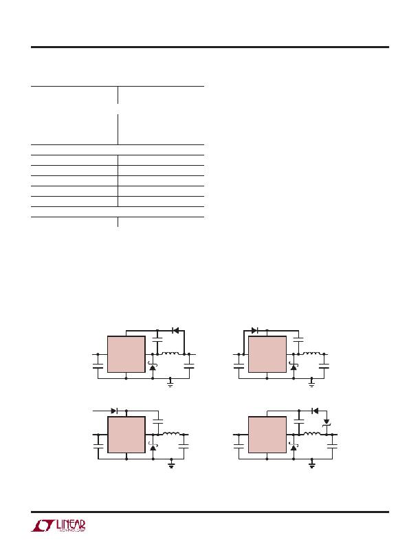
�pin� for� full� ef?ciency.� For� outputs� of� 3.3V� and� higher,� the�
�V� R�
�(V)�
�I� AVE� (A)�
�(A)�
�V� F� at� 1A�
�(mV)�
�V� F� at� 2A�
�(mV)�
�standard� circuit� (Figure� 5a)� is� best.� For� outputs� between�
�2.8V� and� 3.3V,� use� a� small� Schottky� diode� (such� as� the�
�On� Semiconductor�
�BAT-54).� For� lower� output� voltages,� the� boost� diode� can� be�
�MBR0540�
�MBRM120E�
�MBRM140�
�40�
�20�
�40�
�0.5�
�1�
�1�
�620�
�530�
�550�
�tied� to� the� input� (Figure� 5b).� The� circuit� in� Figure� 5a� is� more�
�ef?cient� because� the� BOOST� pin� current� comes� from� a�
�lower� voltage� source.� The� anode� of� the� boost� diode� can�
�Diodes� Inc�
�B120�
�B130�
�B140HB�
�DFLS140�
�B240�
�International� Recti?er�
�10BQ030�
�20�
�30�
�40�
�40�
�40�
�30�
�1�
�1�
�1�
�1.1�
�2�
�1�
�500�
�500�
�530�
�510�
�420�
�500�
�be� tied� to� another� source� that� is� at� least� 3V.� For� example,� if�
�you� are� generating� a� 3.3V� output,� and� the� 3.3V� output� is� on�
�whenever� the� LED� is� on,� the� BOOST� pin� can� be�
�connected� to� the� 3.3V� output.� For� LT3475-1� applications�
�with� higher� output� voltages,� an� additional� Zener� diode�
�may� be� necessary� (Figure� 5d)� to� maintain� pin� voltage�
�below� the� absolute� maximum.� In� any� case,� be� sure� that�
�the� maximum� voltage� at� the� BOOST� pin� is� both� less� than�
�60V� and� the� voltage� difference� between� the� BOOST� and�
�BOOST� Pin� Considerations�
�The� capacitor� and� diode� tied� to� the� BOOST� pin� gener-�
�ate� a� voltage� that� is� higher� than� the� input� voltage.� In�
�most� cases,� a� 0.22μF� capacitor� and� fast� switching� diode�
�(such� as� the� CMDSH-3� or� MMSD914LT1)� will� work� well.�
�Figure� 5� shows� three� ways� to� arrange� the� boost� circuit.�
�The� BOOST� pin� must� be� more� than� 2.5V� above� the� SW�
�D2�
�SW� pins� is� less� than� 30V.�
�The� minimum� operating� voltage� of� an� LT3475� application�
�is� limited� by� the� undervoltage� lockout� (~3.7V)� and� by� the�
�maximum� duty� cycle.� The� boost� circuit� also� limits� the�
�minimum� input� voltage� for� proper� start� up.� If� the� input�
�voltage� ramps� slowly,� or� the� LT3475� turns� on� when� the�
�output� is� already� in� regulation,� the� boost� capacitor� may�
�not� be� fully� charged.� Because� the� boost� capacitor� charges�
�D2�
�BOOST�
�LT3475�
�C3�
�BOOST�
�LT3475�
�C3�
�V� IN�
�V� IN�
�SW�
�V� OUT�
�V� IN�
�V� IN�
�SW�
�V� OUT�
�V� IN2� >� 3V�
�GND�
�V� BOOST� –� V� SW� ?� V� OUT�
�MAX� V� BOOST� ?� V� IN� +� V� OUT�
�(5a)�
�D2�
�GND�
�V� BOOST� –� V� SW� ?� V� IN�
�MAX� V� BOOST� ?� 2V� IN�
�(5b)�
�D2�
�BOOST�
�LT3475�
�C3�
�BOOST�
�LT3475�
�C3�
�V� IN�
�V� IN�
�SW�
�V� OUT�
�V� IN�
�V� IN�
�SW�
�V� OUT�
�GND�
�3475� F05?�
�GND�
�V� BOOST� –� V� SW� ?� V� IN2�
�MAX� V� BOOST� ?� V� IN2� +� V� IN�
�MINIMUM� VALUE� FOR� V� IN2� =� 3V�
�(5c)�
�V� BOOST� –� V� SW� –� V� Z�
�MAX� V� BOOST� ?� V� IN� +� V� OUT� –� V� Z�
�(5d)�
�3475� F05?�
�Figure� 5.� Generating� the� Boost� Voltage�
�3475fb�
�13�
�发布紧急采购,3分钟左右您将得到回复。
相关PDF资料
LT3476EUHF#PBF
IC LED DRVR HP CONST CURR 38-QFN
LT3477EFE#PBF
IC LED DRVR HP CONS CURR 20TSSOP
LT3478IFE#PBF
IC LED DRVR HP CONS CURR 16TSSOP
LT3486EFE#PBF
IC LED DRVR WHITE BCKLGT 16TSSOP
LT3491EDC#TRMPBF
IC LED DRIVER WHITE BCKLGT 6-DFN
LT3492IFE#TRPBF
IC LED DVR HP CONST CURR 28TSSOP
LT3496IUFD#PBF
IC LED DRVR WHT/RGB BCKLT 28-QFN
LT3497EDDB#TRMPBF
IC LED DRIVR WHITE BCKLGT 10-DFN
相关代理商/技术参数
LT3475EFE-1#PBF
制造商:Linear Technology 功能描述:LED DRIVER BUCK PWM 600KHZ 制造商:Linear Technology 功能描述:LED DRIVER, BUCK, PWM, 600KHZ, TSSOP-20
LT3475EFE-1#TRPBF
功能描述:IC LED DRVR HP CONS CURR 20TSSOP RoHS:是 类别:集成电路 (IC) >> PMIC - LED 驱动器 系列:- 标准包装:6,000 系列:- 恒定电流:- 恒定电压:- 拓扑:开路漏极,PWM 输出数:4 内部驱动器:是 类型 - 主要:LED 闪烁器 类型 - 次要:- 频率:400kHz 电源电压:2.3 V ~ 5.5 V 输出电压:- 安装类型:表面贴装 封装/外壳:8-VFDFN 裸露焊盘 供应商设备封装:8-HVSON 包装:带卷 (TR) 工作温度:-40°C ~ 85°C 其它名称:935286881118PCA9553TK/02-TPCA9553TK/02-T-ND
LT3475EFE-1-PBF
制造商:LINER 制造商全称:Linear Technology 功能描述:Dual Step-Down l 1.5A LED Driver
LT3475EFE-1-TRPBF
制造商:LINER 制造商全称:Linear Technology 功能描述:Dual Step-Down l 1.5A LED Driver
LT3475EFEPBF
制造商:Linear Technology 功能描述:Dual Step-Down 1.5A LED Driver,LT3475
LT3475EFE-PBF
制造商:LINER 制造商全称:Linear Technology 功能描述:Dual Step-Down l 1.5A LED Driver
LT3475EFE-TRPBF
制造商:LINER 制造商全称:Linear Technology 功能描述:Dual Step-Down l 1.5A LED Driver
LT3475FE-1
制造商:LINER 制造商全称:Linear Technology 功能描述:Dual Step-Down l 1.5A LED Driver